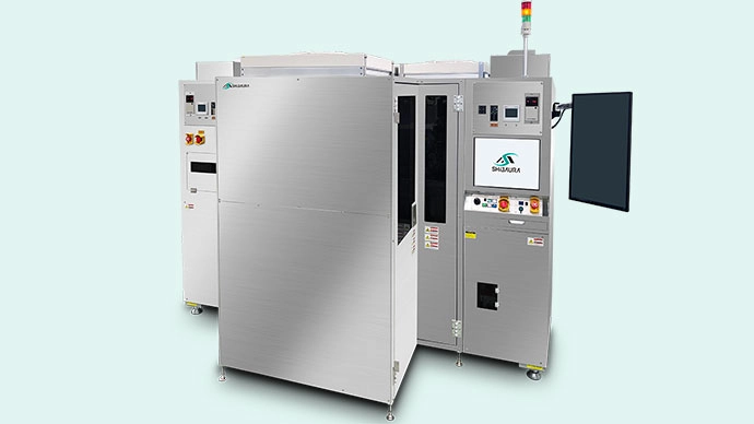
Advanced Package Bonder
TFC-6500-W
High Productivity for Advanced Packaging
A high accuracy and high productivity bonder suitable for advanced packaging.
In the advanced packaging field, which is becoming increasingly important as a core technology supporting the improvement of GPUs used in servers and generative AI, the demands for higher device density and narrower pitch are increasing. Furthermore, chiplet technology, which integrates heterogeneous dies within a single package, has already entered practical deployment and is becoming ever more important. Shibaura Mechatronics has advanced technologies and extensive expertise in the advanced packaging field, supported by a large number of successful installations. The TFC‑6500‑W supports a wide range of packaging technologies—including 2.5D, 2.XD, and 3D integration—and is well suited for mass production. We deliver value to our customers through high accuracy and high productivity optimized for advanced packaging.
We introduce products according to your specific needs!

Features
High Accuracy and High Level Cleanliness
Achieves face down accuracy of ±1μm.
Achieves high level cleanliness (Clean Class 100), contributing to high accuracy and high quality production.
High Productivity
The double-head configuration ensures high productivity.
We also support mass production of diversified packages such as 2.5D, 2.XD, and 3D bonding.
Small Footprint
Compared to the TFC‑6500, it achieves more than double the UPH while limiting the footprint increase to only about 1.3 times, delivering outstanding space efficiency.
Product Explanation
| Main Applications | 2.5D, 2.XD, 3D package products |
|---|---|
| Accuracy | Face Down ±1μm (3σ) *local alignment / R.T conditions |
| Dry UPH | 4,200 or more |
| Chip Size | Max.□30mm |
| Wafer / Substrate Size | φ200 / 300mm Wafer Max.330×320mm Substrate |
| Other | Supports tape feeder / IR inspection / Various bonding processes |
Related Information
Contact Us
- Mechatronics System Division