Wafer Level Package Bonder
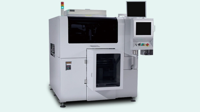
TFC-9000
Supports Processing for Fan Out Wafer Level Package (FO-WLP)
A high productivity bonder suitable for FO-WLP process.
In mobile devices, such as smartphones, the demand for increased energy efficiency and a smaller footprint is rising, leading to greater expectations for the FO-WLP process.
Additionally, when packages become smaller and more highly integrated, it also becomes more difficult to design more connecting internal signals on the chip surfaces. For this reason, more and more package start to use the Fan Out (FO) structure.
Shibaura Mechatronics has over 10 years experiences in sales and production in the FO-WLP field, and has a proven track record with major IDMs, foundries and OSATs. This has helped us accumulate extensive experience and advanced technology.
TFC-9000 contributes to customer's production with "small footprint" and "high productivity" based on an optimized design for FO-WLP.
We introduce products according to your specific needs!
Features
High Productivity With Small Footprint
The double-head configuration and small footprint (main body footprint: approx. 2.5m2) achieve maximum productivity in the smallest footprint.
Supports Both Face Up and Face Down Processes
Adapted for both Chip-1st and Chip-Last (RDL-1st) process. And also supports the face up DAF / Adhesive Sheet, the face down C4 process.
By supporting various processes, it contributes to the improvement of equipment operating efficiency.
Supports Chip on Wafer and Chip on Substrate
In addition to φ200 / 300mm wafers, substrate configurations up to 330x320mm can also be selected.
Product Explanation
| Main Applications | FO-WLP products |
|---|---|
| Accuracy | Face Down ±5μm (3σ) *local alignment / R.T conditions |
| Dry UPH | 7,200 (Global alignment) / 5,100 (Local alignment) |
| Chip Size | Max.□26mm |
| Wafer / Substrate Size | φ200 / 300mm Wafer Max.330×320mm Substrate |
Related Information
Contact Us
- Mechatronics System Division