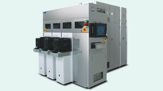
Chemical Dry Etching System
CDE series
Bringing the Endless Possibilities of CDE to the Unseen Aspects of Processing
This isotropic etching system applicable to wafers of φ75 mm to 300 mm has been favoured by customers for many years. While having many achievements for round etching including Si and SiO2, recently this system has also been used for the improvement of device properties by using its remote plasma feature.
It also has a proven track record in transporting and adsorbing SiC wafers, and contributes to the creation of high quality devices with plasma damage-free technology.
We introduce products according to your specific needs!
Features
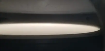
Isotropic Etching
By generating plasma outside of the chamber and performing the etching processing with radical compounds only, this system is capable of perfect isotropic etching processing. It is used for applications such as rounding trench pattern openings and smoothing surface roughness.
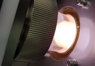
Plasma Damage-Free Feature
Due to the long distance from a plasma to a wafer, the ion generated within the plasma is deactivated and does not impact the wafer. This feature is applied to removal of damaged layers after RIE processing.
Related Information
Contact Us
- Fine Mechatronics Division