Solutions
We Develop Proposals Tailored to Customer Needs, Such As:
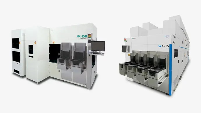
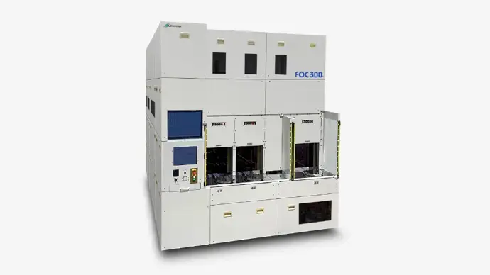
Front-End Process
Nitride Film Wet Etching Technology
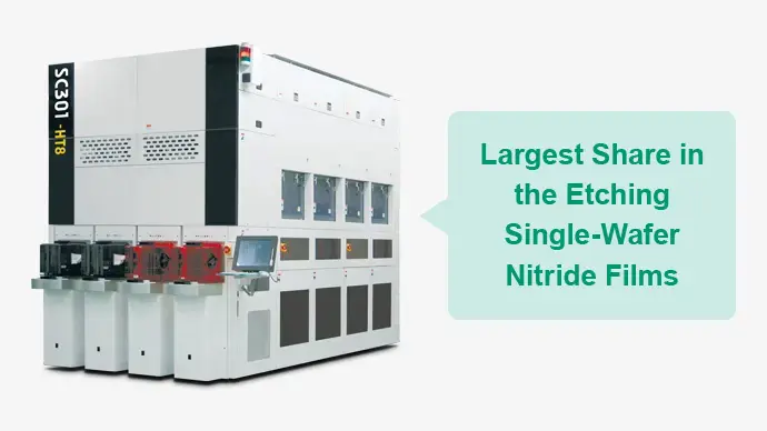
In the nitride film (Si3N4 film) wet etching process, it may be necessary to actively control the distribution of etching amount based on variations in the thickness of the nitride film layer on the wafer surface. However, with conventional batch-type wet etching system, it was difficult to control the distribution of etching amount, which has caused issues.
Shibaura Mechatronics has developed single wafer-type high temperature wet etching system fitted with a wafer proximity heater, and has succeeded in controlling the distribution of etching amount on the wafer surface depending on the heater settings.
This contributes to improved semiconductor device performance and yields.
Nitride Film Wet Etching Technology
In the nitride film (Si3N4 film) wet etching process, as the underlining layer is subjected to a small amount of etching if the entire nitride film on the wafer surface is etched, the amount of etching can cause problems. Especially when used phosphoric acid is recovered for reuse, when the Si concentration within the phosphoric acid changes, the amount of etching on the underlying layer also changes.
Shibaura Mechatronics recycles used phosphoric acid and has added a new feature that controls the Si concentration within the phosphoric acid it uses. This enables the amount of etching of the underlying layer to be kept to a minimum.
Wafer Cleaning Technology
There are two types of wet cleaning system that affect the cleanliness of wafers, batch type and single-wafer type. While the batch type has the benefit of processing multiple wafers at once, it also comes with issues, as it is easier for the surface roughness of the wafers to deteriorate, and cleaning performance is prone to instability.
Shibaura Mechatronics uses the single-wafer type, enabling alternating processing with ozone water and dilute hydrofluoric acid, which is difficult with the batch type. As a result, the amount of etching on the surface of the wafer after cleaning can be finely controlled, suppressing deterioration in surface. Furthermore, the impact of mist in the processing chamber is mitigated by enhancing exhaust efficiency while ensuring an optimal, stable cleaning performance.
Plasma Damage-Free Etching Technology
To improve the electrical properties and yields of devices, in the dry etching process customers often wish to perform etching that does not produce plasma damage such as ion impact, light or charging, or to remove plasma-damaged layers after etching. Shibaura Mechatronics' CDE system employs a remote plasma mechanism that isolates the plasma generating component from the etching processing component, enabling plasma damage-free etching and the removal of plasma-damaged layers. Leveraging this feature, we have an extensive track record of mass producing image sensors as well as Si or SiC power semiconductors in the field.
Photomask Etching Technology
In the photomask manufacturing process for semiconductors, it is necessary to perform uniform and high accuracy etching over the entire surface to deal with patterns that involve a mix of various wiring dimensions and wiring densities.
Shibaura Mechatronics enables uniform etching across the entire pattern surface by employing a unique structure in the plasma generating component using in etching, and a function that controls plasma distribution. In addition, high accuracy etching is achieved by introducing a large amount of the gas used for etching and venting it in large volumes.
Photomask Etching Technology
When fine particles generated during etching adhere to a photomask, they can be transferred onto the photomask pattern and cause a direct defect, something that cannot be resolved through cleaning after the etching process. This is why it is necessary to prevent fine particles from being generated during etching.
Shibaura Mechatronics maintains the inside of its system in a clean state through features that remove deposits that form on the etching processing components and vent airborne particles. In addition, the inner surface of etching processing components are coated with materials that are resilient to etching and corrosion, in order to suppress the formation of fine particles due to damage from etching.
Photomask Cleaning Technology
If there is a defect in even one place in the wiring pattern of a photomask, which serves as the exposure master plate, that defect will be transferred to all of the exposed wafers. For this reason, at photomask manufacturing sites the cleaning process is repeated to ensure the removal of foreign particles that could cause defects. However, if powerful cleaning methods are employed, the issue of pattern damage where defects form in the wiring pattern of the photomask can occur, and to date, there have been limitations to the removal of fine foreign particles.
Shibaura Mechatronics has newly commercialized a freeze cleaning technology that can remove ultra-fine particles without damaging patterns. By utilizing a property of water that causes it to expand in the process of freezing, foreign particles can be selectively lifted and removed from wiring patterns. Moreover, since water is used for cleaning, it helps reduce the cost of chemicals and minimizes the environmental impact.
Lamp Heater-Integrated Vacuum Drying Technology
In the cleaning process, it may be necessary to clean the door latch mechanism in addition to the internal parts that face the wafer. For latch mechanisms, which have complex structures that are hard to dry, we use vacuum drying combined with our lamp heater to evaporate and fully dry internal water droplets.
In addition, by processing cleaning and drying using separate tanks, idle time is significantly shortened, leading to high throughput.
Coarse Cleaning Function to Deal with Heavy Dirt
FOUPs or FOSBs brought in from outside a plant may have large amounts of dust or heavy dirt stuck to the outside. If they are placed in conventional cleaning unit as-is, the cleaning tanks could become dirty, reducing cleaning performance and creating issues. That is why in some cases they are lightly rinsed before being placed in a cleaning unit by hand. To deal with this issue, solutions such as setting up self-cleaning functions for cleaning tanks and periodically cleaning the tanks have been considered, but this is problematic in terms of reduced throughput and utilization rates.
Shibaura Mechatronics has made it possible to add a dedicated processing tank (course cleaning tank) which performs cleaning at the time of receipt. After unpacking a FOUP or FOSB received from an external source, it can be placed in the unit as-is. Rinsing it once in the course cleaning tank prevents the main cleaning tank from becoming dirty, and allows the cleaning process to continue without requiring self-cleaning time.
Function to Check the Level of Cleanliness After the Cleaning Process
Although regular cleaning is performed, verifying the level of cleanliness achieved and that the targeted particles have been removed has required regular cleanliness checks using separate inspection system.
Shibaura Mechatronics has made it possible to equip measurement functions to gauge particle count, outgassing types and amounts, humidity and other variables in order to periodically check cleanliness levels.
In-Unit FOUP Buffer Function
With the performance of wet cleaning system improving, it has become possible to achieve high throughput. However, overhead hoist transport (OHT) used to transports FOUPs within a plant is not able to load and unload FOUPs based on the timing of wet cleaning system. For this reason, it was not possible to demonstrate the true throughput performance of wet cleaning system.
Shibaura Mechatronics prepared buffer stages at both the load and unload sides to avoid lowering the effective throughput. This makes it possible to load and unload based on the timing of the OHT system, achieving the true high throughput of the system.
Low-Temperature Ashing Technology
In the process for patterning thinned wafers, some customers wish to process wafers with the protective and support materials still attached.
Shibaura Mechatronics has combined the use of high-density plasma source with electrostatic chucks to enable ashing under low pressure and low temperatures.
In recent years, this feature has been utilized to build up a track record removing cured resist remaining on thin wafers with protective and support materials, contributing to improved productivity.
Back-End Process
IC Chip Pickup Technology
As memory chips have become progressively thinner, a possibility for damaging chips arises when they are picked up from the wafers, attributing to an increase of a fraction defective and productivity deterioration.
Shibaura unique chip bonder, which applies a chip pickup method suitable for thin chips, can reduce the damage to the chips even thin chips.
High Accuracy IC Chip Bonding Technology
The next-generation of competitive integrated high performance devices demand increased device density, which make the Chiplet architecture became important in the semiconductor back-end process. SiP (System in Package) that optimally combines different types of chips is required. In order to combine chips with high integration, the chip bonder with stable high accuracy became important. In general, due to the effects of thermal expansion it is not easy to maintain a stable high accuracy repeatability with a high speed movement. This is even more difficult in the FO-PLP process, which uses large size panels.
Our chip bonder is equipped with a function that automatically detects and corrects postural deformations at process points during production operation. This enables both a stable chip bonding accuracy and a high production capacity.