Search by Semiconductor Manufacturing Process
This Is an Introduction to Shibaura Mechatronics Products and Services Based on the Semiconductor Manufacturing Process
Shibaura Mechatronics Supports Everything From the Front-End to Back-End Processes!
| Front-End Process |
|
|---|---|
|
|
|
| Back-End Process |
|
|---|
Front-End Process
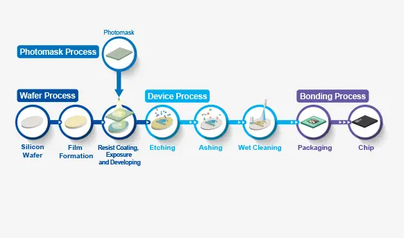
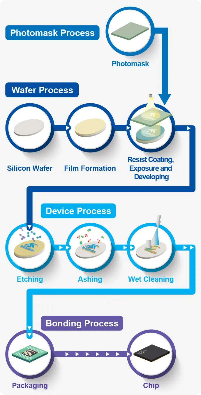
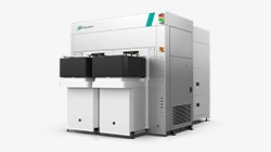
Wafer Process
Many semiconductor products use thin discs (silicon wafers) cut out from high-purity silicon as the base material. A semiconductor product is completed after undergoing a vast number of processes, but the silicon wafer used as the basis requires very high levels of cleanliness.
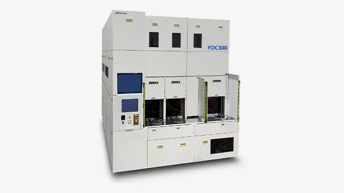
Shibaura Mechatronics offers single-wafer cleaning system supporting a wide range of processes to achieve this high level of cleanliness.
Device Process
After a photomask circuit or pattern has been transferred to a resist, steps such as development, etching and ashing are repeated to remove unnecessary parts from the circuit or pattern.
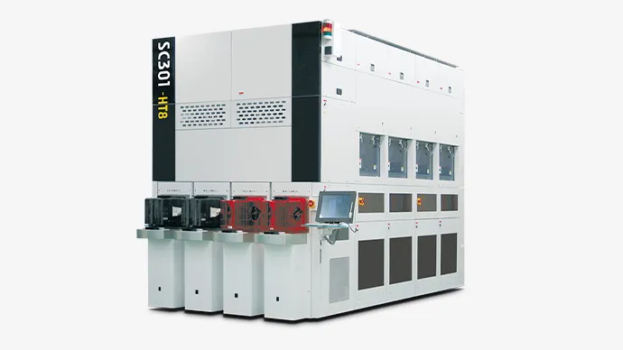
Shibaura Mechatronics has a range of etching system and ashing system that contribute to device reliability and improved yields.

Photomask Process
To create the required circuit or pattern on a wafer, first the designed circuit or pattern is drawn on the surface of a glass plate. Then an exposure device is used to project light onto the resist-coated surface of the wafer to transfer the design.
The glass plate on which this circuit or pattern is drawn is referred to as a photomask. If a photomask has defects, those defective parts will be transferred onto the resist.
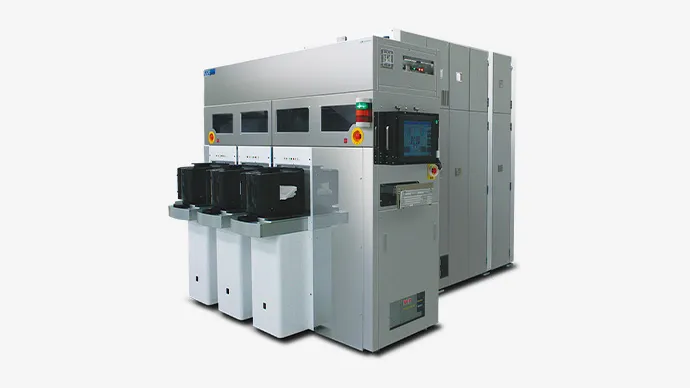
Shibaura Mechatronics provides a range of etching system and wet cleaning system that facilitate defect-free photomask manufacturing.
Package Process
In advanced packaging, wet processes such as cleaning and etching are indispensable for steps that include RDL formation and glass core substrates.
During the middle-end process and back-end processes, where semiconductor chips are mounted on substrates or interposers for connection and protection, performance equivalent to the front-end process level of wafer is required.
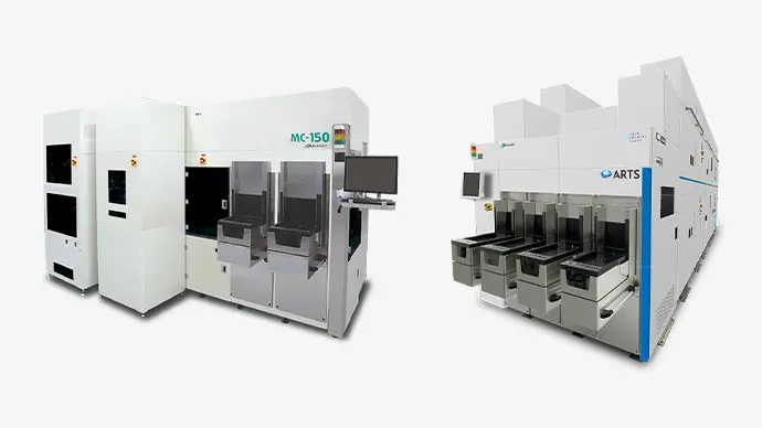
Shibaura Mechatronics offers panel spin systems applicable to various wet processes, including high levels of cleanliness and etching, for advanced package.
Back-End Process
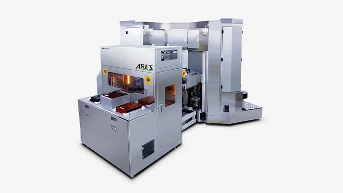
Bonding Process
With developments such as IoT, 5G and AI, semiconductor products request higher performance and reduced latency.
However, it is believed that miniaturization, which involves narrowing circuit line widths and integrating even more circuits and patterns on a single chip, is reaching the physical limitations.
Under these circumstances, there is a growing trend toward improving the performance of semiconductor products through back-end packaging technologies, such as combining multiple chips in a single package.
Shibaura Mechatronics offers a range of high accuracy bonders which can support various kinds of processes and packages.