Sputtering Equipment for Research and Development
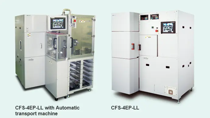
CFS-4EP-LL
The Industry's Leading Supplier of R&D Sputtering Equipment
These units can be used for a variety of film formation applications, from R&D to Variety production and low-volume production.
Applications
- Semiconductors, electronic components, LEDs, LDs, sensors, wafers, MEMS, etc.
Typical Film-Forming Materials
- Dielectric Film etc.
AlN, SiN, SiO2, ZrO, TiO2 - Transparent Conductive Film
ITO, ZnO - Metal Film etc.
Au, Ag, Cu, Si, Ti, Sn, Cr, Al, Ni, DLC
Features
- Extensive delivery track record
We have delivered many units to universities, research institutions, and companies, and they are active in cutting-edge research fields.
- Fully automated operation
Fully automated operation is possible simply by setting the program.
- Versatile of options
These units support automatic conveyance, automatic variable distance from target to substrate, simultaneous sputtering and bias sputtering, etc.
CFS-4EP-LL Specification
| Processing Method | Load lock type |
|---|---|
| Sputtering Method | Side |
| Table | Orbital table |
| Sputtering Source | Up to four (normal and strong magnetic fields selectable) |
| Data | Data logger |
| Co-Sputtering | Supported |
| Bias Sputtering | Supported |
| Table Temperature Control | Max. 600℃ heating / water cooling |
| Variable Distance from Target to Substrate | Supported |
| Automatic Feeder | Supported |
Related Information
Contact Us
The Division in Charge of This Product
- Mechatronics System Division